↓ What is nano3DSense?
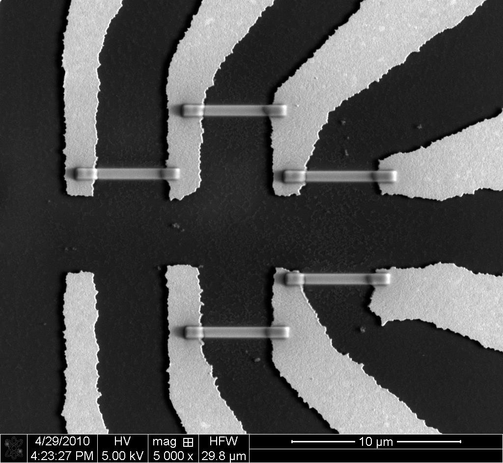
nano3DSense is a patented maskless lithography process with nanometer precision for the 3D printing of novel sensor-active nanomaterials on custom-tailored substrates (tranducers or microchips). The novel sensor-active nanomaterials allow for advanced measurements of a broad range of values, such as force, pressure or displacement by a simple electronic readout on a micro chip.
Image: sensor-active nanomaterials (nano3DSense) printed on a substrate containing metallic electrodes.
In contrast to conventional top-down methods, which require complexe cleanroom-technology, nano3DSense is a single-step lithography process, that can be beneficially used for easy and fast manufacturing of 2D and 3D sensors.
As nano3DSense does not require silicon processing technologies (such as photo masks, exposure, wet chemistry, etc.), more than 250 cleanroom steps can be avoided. nano3DSense is best suitable for adaptive series production, rapid prototyping and in R&D.
↓ Why did we develop nano3DSense?
Conventional micro sensors (e.g. optical, piezo-electrical, piezo-resistive, and capacitive methods) reach their physical limits in many applications with respect to their miniaturization and accuracy potential already today.
In the case of optical detection e.g., the diffraction limit of the laser, which cannot become smaller than 1.4 µm (HWFM, “Half Width at the Full Maximum”), represents a fundamental barrier for further miniaturization of the optical setup.
The situation is very similar for other sensors, such as piezo resistors or capacitive methods. As they require complicated cleanroom technologies or silicon doping processes, the miniaturization potential is usually exhausted at dimensions of 20–50 µm.
Regarding transducer material selection, traditional sensors are mostly restricted to silicon, and cannot handle more than two dimensions (2D).
With nano3DSense, there are virtually no limits with respect to miniaturization, accuracy and transducer material selection. If needed, sensor sizes below 10 nm are achieved by a simple 3D printing procedure.
↓ Why is miniaturization even important?
- Miniaturization allows for smaller sensors, which are more suitable for detecting microscopic objects or quantities. The performance (e.g. sensitivity and signal quality (signal-noise level)) is also normally increased, when sensors become smaller.
- For special applications with high data volumes (e.g. multiplex-arrays, realtime force measurements) the signal processing speed (or throughput can be increased when sensors are minaturized.
When space is tight and installation restricted (e.g. with respect to minimally invasiveness), the nano3DSense sensor comes into its own. With the same measuring range and higher signal performance characteristics, the nano3DSense transducer is up to hundred times smaller in construction than a comparable piezo resistor.
↓ Why is the nano3DSense sensors up to 500 times more sensitive than a conventional semiconductor sensor?
The sensitivity of nano3DSense can be flexibly tuned to your measuring requirements simply by geometrical design benefits or proper material choice. An external force that causes a small displacement on a substrate (e.g. pressure diaphragm or force-feedback beam (cantilever)) is described by Stoney’s formula (picture below). The displacement, which is a good measure for the sensitivity, strongly depends on the Young’s Module E (material stiffness) and the substrate’s thickness.
By aligning geometry and material stiffness parameters (table below) a sensitivity that is up to 550 times higher compared to an conventional semiconductor piezoresistor can be achieved using nano3DSense. Conventional semiconductor piezoresistors don’t show such benefits since they require a complicated doping process and silicon as a base material, which limits the minimum achievable thickness of the substrate (typically 1-3 µm) .
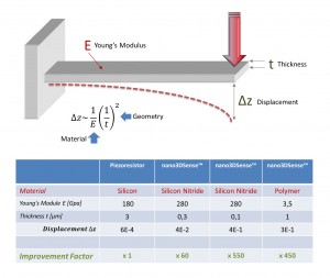 Image and Table: The displacement Δz of a cantilever beam due to an external force strongly depends on thickness t and the Young’s Modulus E of the material (Stoney’s formula). With softer and thinner materials the sensitivity can be drastically increased (table).
↓ Does nano3DSense provides a stable sensor signal? (When compared to conventional sensors)
nano3DSense force, pressure and strain sensors are durable high-precision measurement devices which possess exceptional characteristics for measurements in the long term or short term, whether for high frequency dynamic or static measurement events. A nanosensor fabricated with nano3DSense 3D printing technology is a highly robust nanocomposite material which normally consists of nanogranular metallic clusters, randomly embedded in a carbonaceous matrix (like a cermet, a composite material composed of ceramic (cer) and metallic (met) materials).
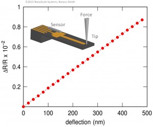
Ideally designed for demanding requirements
The nano3DSense sensor is ideally designed to meet optimal sensor requirements, such as temperature resistance and hardness, the flexibility to undergo elastic deformations and very stable electrical characteristics. Pictures below, for instance, show stability curves which have superb characteristics in the short time and long-term (degradation curves). E.g. when operated as a full bridge of four identical nano3DSense sensors excellent linearity and – thanks to their small sizes – very low power consumption can be achieved. Additional interference effects such as temperature variations can be avoided efficiently without any further compensation efforts.
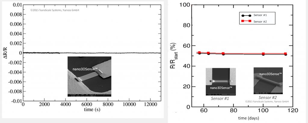
Proven in Harsh, Rugged Environments
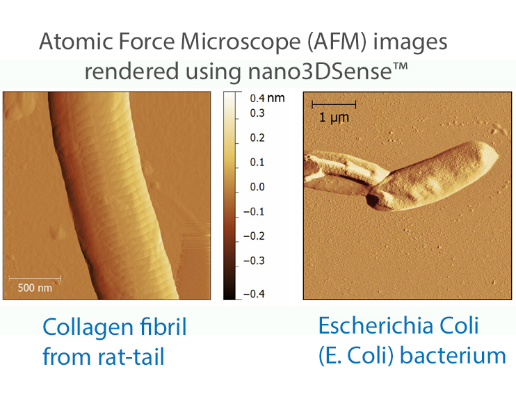
The nano3DSense has been designed and proven as a rugged and high-performance sensor platform in many critical and highly sophisticated applications, for example in atomic force microscopy (AFM). Pictures below show AFM image scans taken and rendered with the nano3DSense force sensor that was fully integrated on a commercial AFM micro cantilever. To perform in atomic force microscopy an integrated force sensor must withstand great mechanical and electrical loads. Since the cantilever is operated with very high mechanical oscillation frequencies (>1 MHz) it must perform many billions of deflection cycles during a single image scan. The nano3DSense can be operated effortlessly under these and other harsh environments (e.g. fluids, high temperature > 500°C) with excellent performance in terms of durability and short or long-term stability.
For more information read our article published by “Nature” in the September 2016 issue of “Nature Communications” magazine.
↓ Can the nano3DSense Sensor be mass produced?
Yes. nano3DSense is a fully automated batch process which allows consistent production of hundred thousands of sensor per year with a single production tool. Our patented 3D nanoprinting process was designed from scratch to meet highest quality standards, such as reproducibility and consistency.
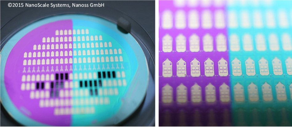
Image: nano3DSense force and pressure sensors can be mass fabricated using fully automated batch procedures on wafer level with highest possible quality standards
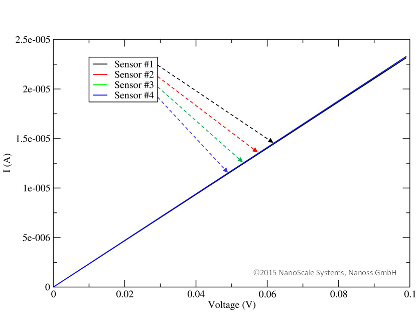
Image: We put highest possible standards on consistency in the sensors batch fabrication process
↓ What does platform technology mean and how is nano3DSense integrated into my application?
nano3DSense was developed and optimized as a multi-purpose sensor platform and for numerous applications in force, pressure, strain, and other MEMS/NEMS sensors.
Wherever miniaturization and adaptivity to the measuring environment in industry and R&D are crucial, the advantages of nano3DSense can be used the most. Thanks to the high adaptivity, even difficult measuring tasks can be completed as well, which cannot be solved using traditional methods or with high effort only.
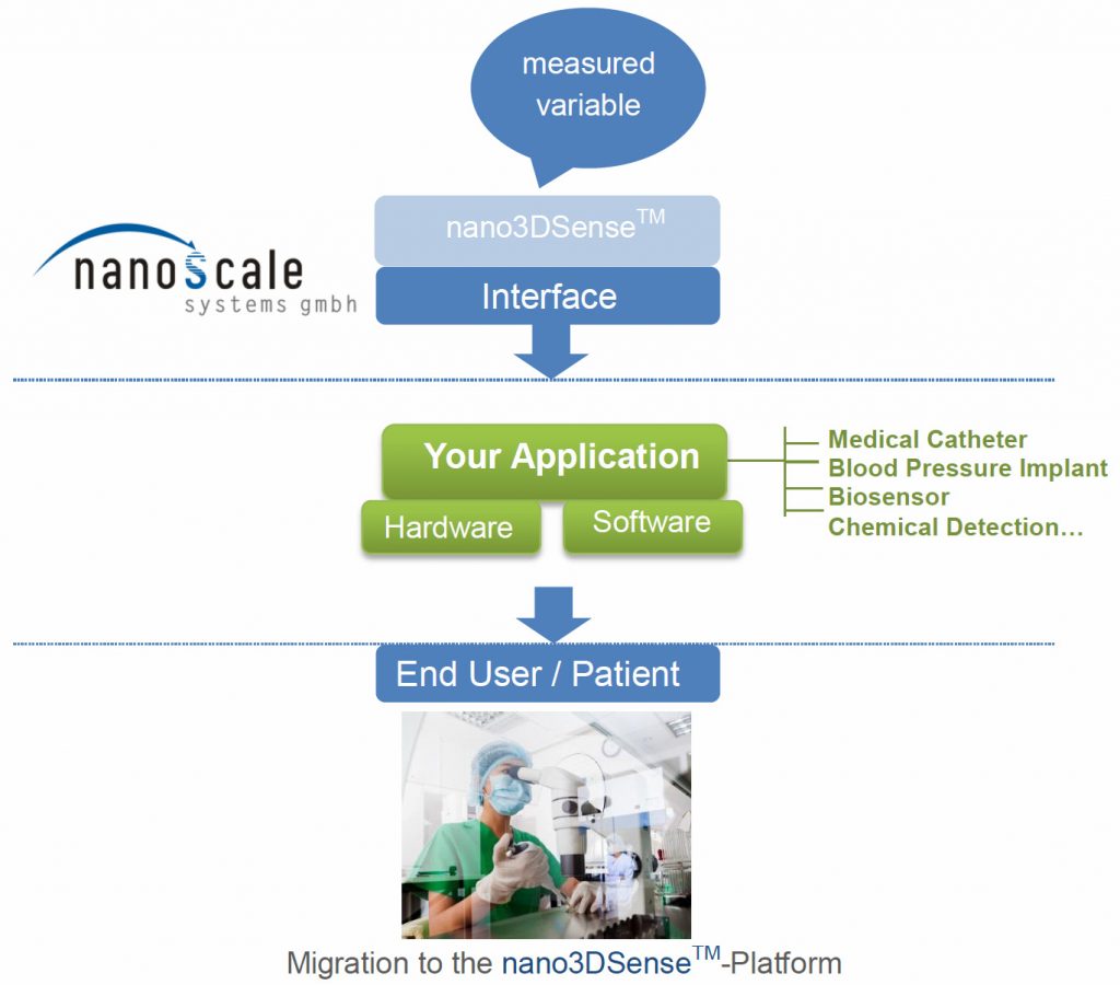
nano3DSense is a flexible signal transducer between measured variable and the applications of our customers (see graphic).
With the help of physical interfaces, which we define together with our customers, we establish a dedicated bridge optimally connecting the central measuring requirements of the end customer with the applications (hardware and software) of our customers.
You have more questions but can’t find an answer? Please contact us for our help and support.
Read more:

