
How does 3D Nanoprinting for Sensors Work?
More than 250 complex processing steps in cleanroom technology – from CAD design to the finished product – are eliminated without compromises: Consequently turning away from traditional semiconductor and silicon processing technologies (such as lithography masks, resists, and cleanrooms), nano3DSense allows us to bypass multiple complex and expensive production steps for microelectronic components such as sensors and to revolutionize the entire production process.
For the first time, our micro components are directly printed three-dimensionally (3D) with true nanometer precision on a customer-specific substrate and are there immediately operational e.g. for sophisticated force or pressure measurements. In contrast to the traditionally known lithography, thanks to 3D Nanoprinting, the achieved results can also be used to drastically improve and simplify the sensor design, which otherwise would require an elaborate measurement setup.
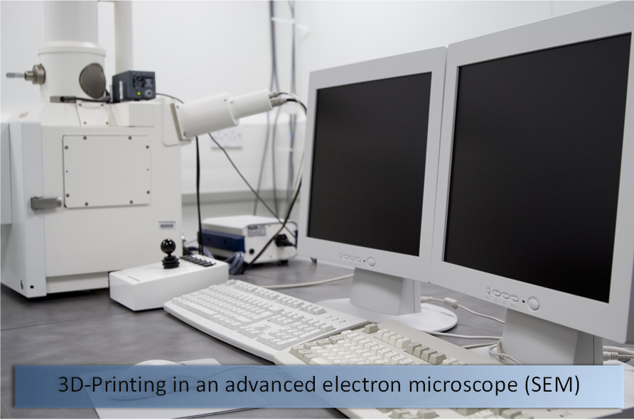
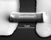
3D-Nanoprinting in an advanced electron microscope (SEM)
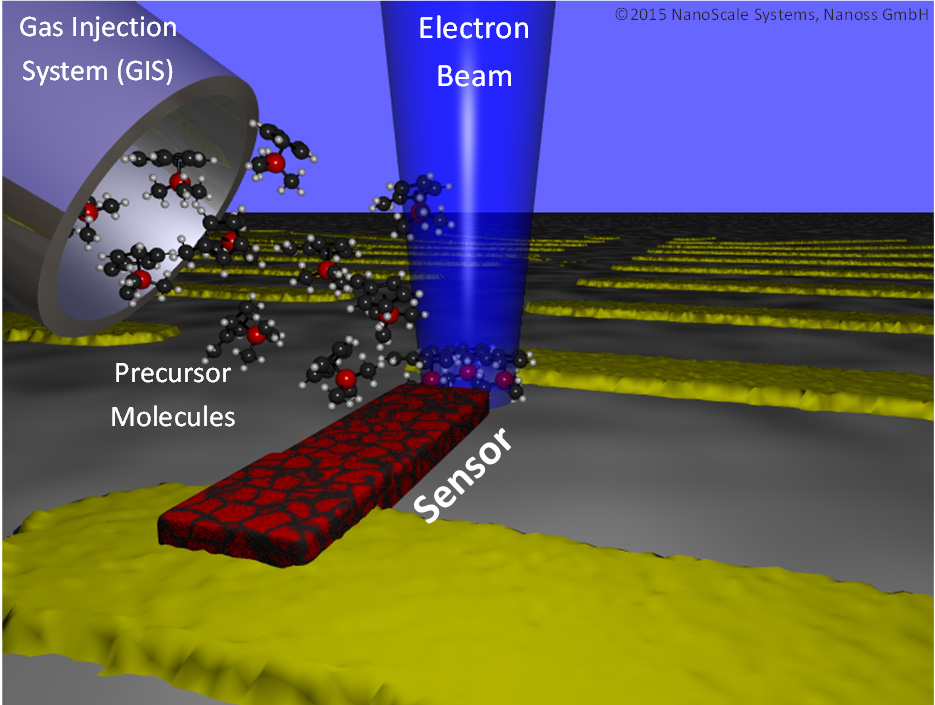
How the Nano 3D-Printer works together with electron beam, gas injection system (GIS) and precursor
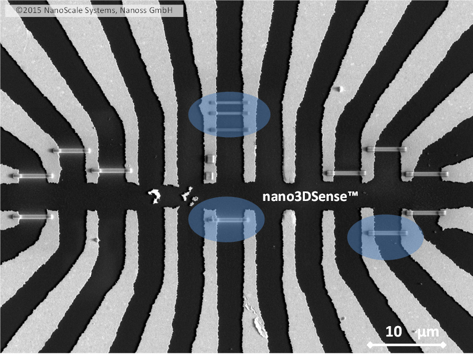
Print sensors flexibly with highest possible precision everywhere on an integrated circuit

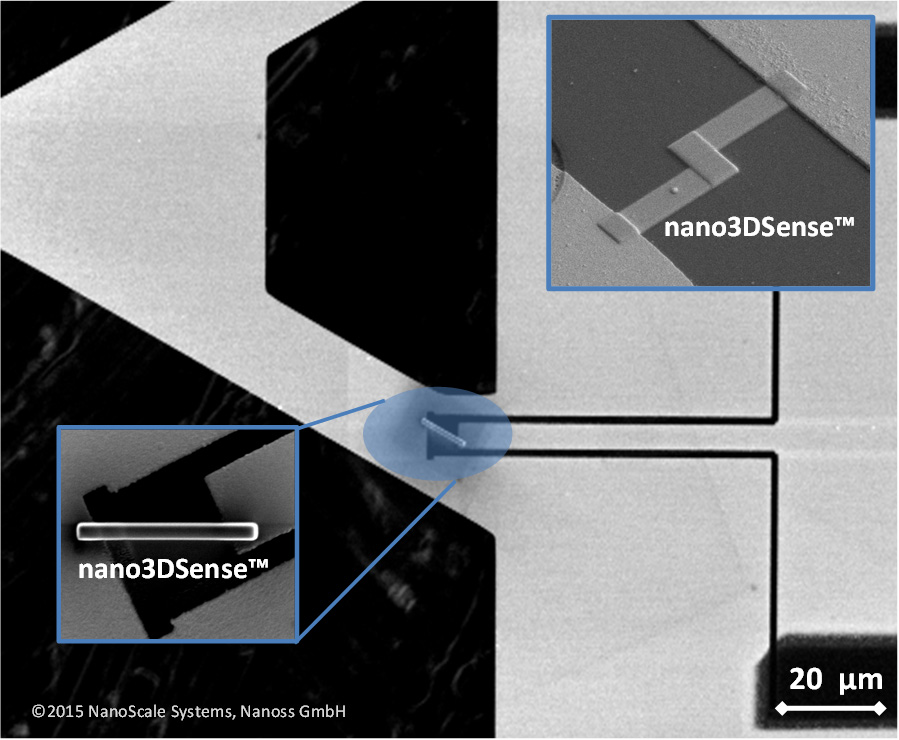
Rapid Prototyping: The sensor can be applied with highest possible precision on all surfaces or materials without any prior preparations.

Force- pressure- and strain measurements with highest possible resolution on any surface
Free selection of sensor geometry and size: it takes only seconds
nano3DSense is a maskless lithography process that does neither require a cleanroom nor silicon, thus giving unparalleled flexibility and precision for your application

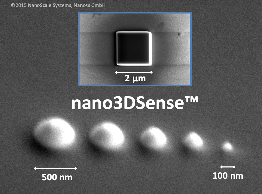
3D-Printing with True Nanometer-Precision
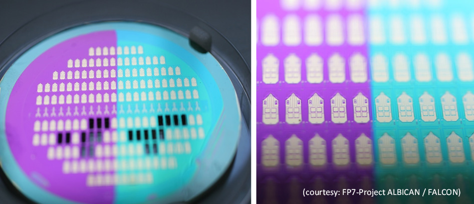
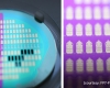
nano3DSense ist fully automatable and can be used for fast batch production even on wafer level.
Nanometer Precision for Production and Rapid Prototyping
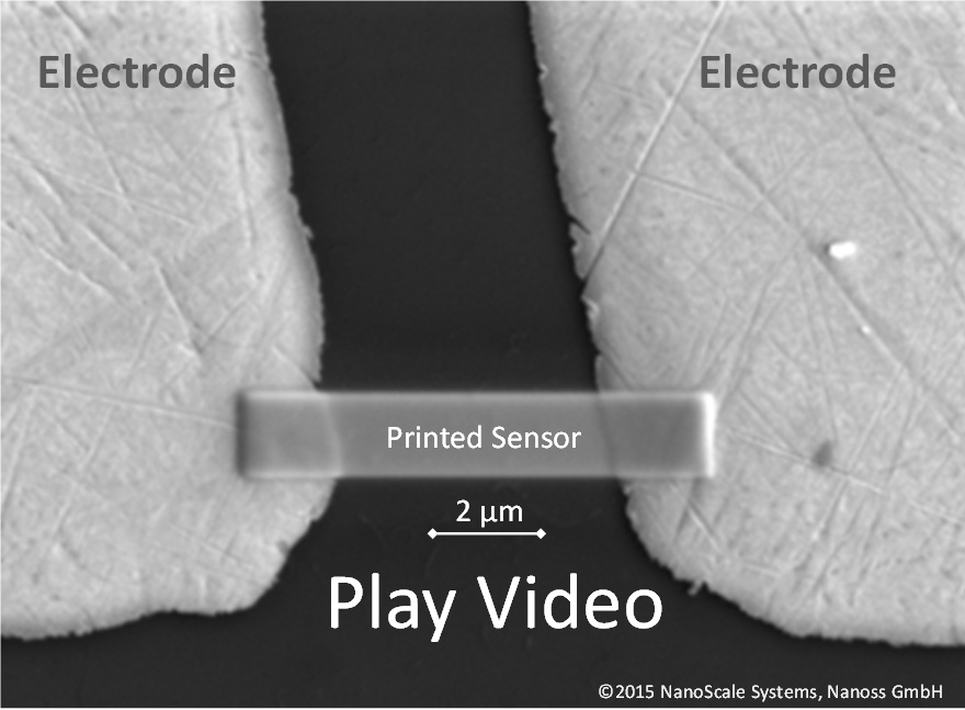
3D Nanoprinting is used in modern scanning electron microscopes (SEM) that are fully adapted to nano3DSense . There, a highly focused electron beam with a diameter of a few nanometers only is available in high vacuum for 3D printing. This beam is used as an ultra-tiny “pen” for the layer-by-layer production process of sensors. We achieve unbeatable small dimensions, which allow sensor sizes below 10 nanometers if required. And this on almost all material surfaces or geometrical shapes (see video above).
The groundbreaking flexibility of our method allows e.g. the provision of quickly adjustable production series or the fast implementation of tailored rapid prototyping requests in R&D for our customers in a cost-effective and unrivaled manner.
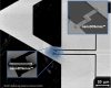
Click on image below to start a realtime video demo for the manufacturing of a nanosensor using 3D nanoprinting with nano3DSense
Read more: